AGBTs Past
We now have a Discord! There’s been some interesting chat and there’s an AGBT channel for those wanting to use that to coordinate. Click here to join. I’m also posting a few clarifications from Spike at Oxford Nanopore over there!
When I think back to AGBTs past two events stand out. The first is Clive’s 2012 Oxford Nanopore talk. The Oxford Nanopore “Mother of all Demos” if you will.
Here they announced a (then impressive) 4% error rate on nanopore sequencing!

The full deck is available online, and it’s well worth a look!
The second is the iconic release of the Ion Torrent PGM at AGBT 2010! A release which was somewhat light on details but had a strong sense of show-person ship.
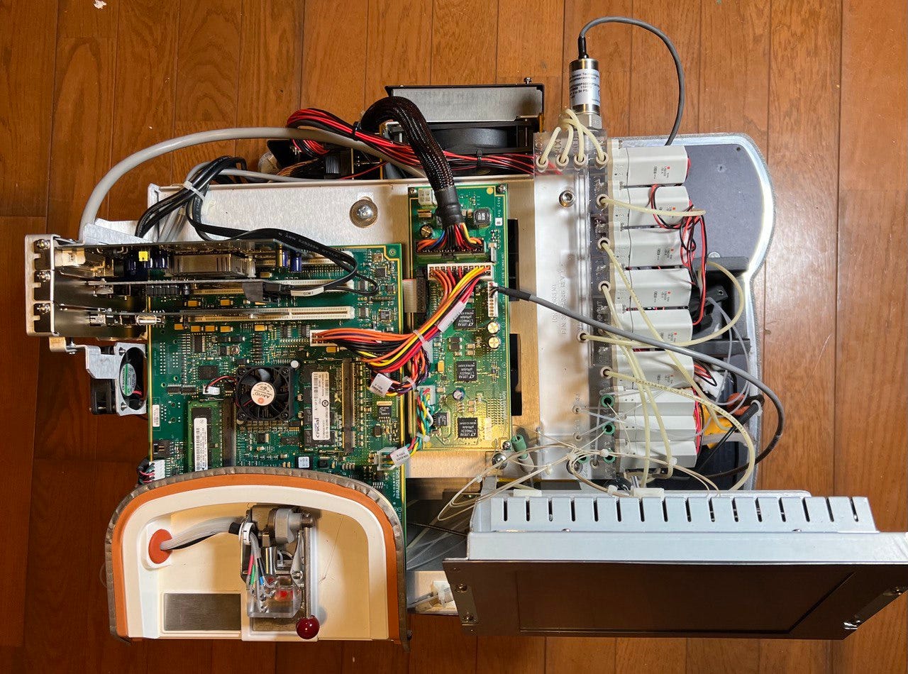
So, in celebration of AGBTs past, let’s tear apart an Ion Torrent PGM!
Removing the chassis reveals a reasonably elegant design. Certainly better integrated than the original Solexa/Illumina Genome Analyzer, which was a thrown together lab rig. But still showing clear signs of first generation product, like the consumer grade PC power supply, and Apple USB Sync cable glued to the case (it came with an iPod you know!)
With the case off everything is clearly accessable. The system looks like a standard PC. And it appears to use PCIe cards (in somewhat odd slots) and the display is just a OEM VGA monitor with serial touch screen interface.
However, this is very much not a standard x86 motherboard. It is in fact it’s a custom design built around a 333Mhz PowerPC (MPC8560) as was the style at the time:
The CPU is coupled with 3 Lattice ECP2 (1 LFE2M50 and 2 LFE2M20s) FPGAs and a 1GB and 4GB RAM sticks.
For the time, these would be reasonably powerful FPGAs. They are capable of data rates of up to 3Gbps, or more realistically 840 Mbps over LVDS.
I’ve looked at Ion Torrent raw signal data in the past, this reference suggesting that it was sampled at 15Hz more or less matches my memory. That’s a data rate of 240 bps at 16bits per sample. I don’t remember what the resolution used on the Ion Torrent was exactly, but they certain need a lot of it. The true incorporation signal is a tiny little blip on a huge background, so a lot of dynamic range is required:

If we therefore assume they used 32bit samples, we’d be looking at 480bps. This would give 1.75M wells per LVDS pair. Each ECP2 appears to be capable of hosting 32 pairs. This would let us address 56M wells per FPGA, or given that we have at least two of them which appear to be closely coupled to the device (there might be another hiding under the drip tray) 112M wells.
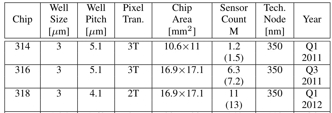
As it stands the PGM scaled to 11M wells, and stuck to 3 micron well sizes:
As we saw in the previous post, after the PGM Life scaled well sizes down significantly to sub-micron sizes:
Given the physical die size used in the PGM using these feature sizes you certainly should have been able to scale beyond 11M reads, you could probably physically pack more than 300M in the available die space. FPGA bandwidth was available for ~100M sensors/reads.
Of course you’ve still got to get that data out of the FPGA and into the buffer (likely the 4Gb RAM stick), and then over to the CPU. Then onto the internal HD and finally over (gigabit) Ethernet to the Ion Torrent server. This would all have been fairly troublesome and required significant data reduction.
One question that came up on twitter is if the PGM could have scaled to larger chips/more reads. I would say that the answer is almost certainly yes based on the above.
However it’s also clear that this was a first generation product, it would have been a pain to scale much further, and they probably wanted to do a re-design anyway. So instead in 2012, Life announced the Ion Proton along side the release of the final PGM chip, the Ion 318.
I might do a follow up post on the fluidics system at some point (which seems pretty standard) but in the mean time, there are more pictures over on discord.


