Nanopore Array Fabrication
I recently wrote about biological nanopores and touched on the fact that the seemingly relatively low margins on nanopore sequencers are likely related to the novel fabrication processes used.
This prompted a few interesting conversations, and I thought in this post it would be fun to review a patent from Oxford Nanopore, covering array fabrication approaches.
Electrodes
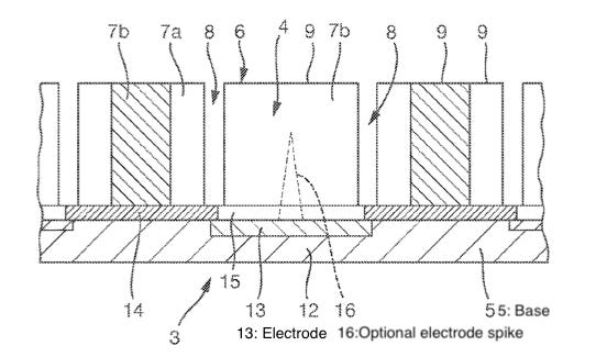
The patent suggests that Silex were used to fabricate electrodes on a 6 inch Si wafer. Other patents give a better sense of the wafer structure:
Here we have platinum electrodes with through wafer interconnects. This allows the electrodes on the top surface to be routed through the substrate and out of the bottom of the wafer where they can be bonded to an ASIC (in the case of the MinION) or pins (Flongle). This looks rather like a TSV (Through Silicon Via) process.
The use of Platinum perhaps explains why a MEMS fab (Silex) is being used here rather than a more standard process, where typically copper or aluminum would be used on metal layers.
Nanopore experiments in academia usually use silver electrodes, however as noted silver is “difficult to incorporate in a silicon wafer manufacturing process due to its tendency to undergo oxidation on exposure to light, air and high temperatures”. So isn’t a good option here…
Patents also describe an optional electrode spike, but while Silex have some cool patents around fabricating micro-needles, this seems challenging, and doesn’t seem to be mentioned elsewhere in the patent…
Membranes and Structures
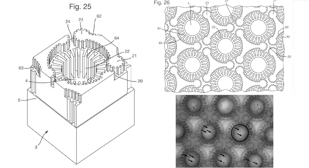
The substrate described above, contains the basic electrode structure. Droplets need to added to the array into which nanopores will be inserted. These droplets need to be confined above electrode. A structure sits above the electrode to enable this.
These structures are formed using SU-8 (Seed layer) and TMMF 2030 dry-film resist (Pillar structure):

Well Sizes and Pore Lifetime
The patents notes that the experiment/pore lifetime is related to the volume of the droplet. The graph below would suggest that a MinION (with a 72h run time) uses droplets in the 175 micron range:
It also suggests that if you try and cram more pores onto a chip, and in doing so reduce droplet size, flow cell lifetime will decrease. This may limit options in terms of increasing pore density to push throughput.
How Much does this all cost?
Beyond ONTs annual reports (which show margins in the 50% range, and therefore suggests a ~$45 COGS on a Flongle flow cell) I don’t have a good estimate for the cost of the above process.
However, a COGS analysis from first principals would be interesting. This would let us better estimate how cheap a Flongle type device could be manufactured at scale.
The Flongle array looks to be somewhere in the region of 10mm square, this may be somewhat limited by mechanical constraints, as it seems like 126 wells should fit on a substrate less than a quarter of this size easily.
I plan to continue to try and figure out how to estimate COGS at scale for the above process. But if you have any thoughts please get it touch! (new@sgenomics.org or twitter).


