The MinION Flowcell - Nanopore Sequencing: An Introduction
My apologies to readers more interested in technical content, we’re going to be heading back to that content for a while now.
Someone over on LinkedIn suggested I start a Patreon so I have. Donations are most welcome, but not required or really expected…
Anyway, as mentioned in the last post where we looked at the MinION device, I’ve been looking at Deamer’s excellent book on Nanopore sequencing. This contains a lot of pretty specific information about the MinION. Actually, I note that the section I’ve been referring to is written by Oxford Nanopore’s James Clarke. Hi JC, hope you’re doing well.
The exploded view of the flow cell looks nice, but doesn’t reveal anything non-obvious:
But MinION flow cell PCB is a little more interesting. Here you can see the ASIC and sensor array bonded to opposite sides of the PCB:
“ASIC is bonded to the lower side of the flow cell's PCB substrate with connections through to the upper side where the sensor array is mounted to ensure a short connection path with minimal parasitic capacitance.”
That’s pretty neat, I imagine some effort must have gone into getting the routing “just right” it also suggests that ASIC and sensor array layout need to be coordinated. This will likely make doing design revisions on each component a massive pain. For example, if you want to move to a higher pore density it seems like you’d also have to re-spin the ASIC to match and vice-versa.
It’s also weird that the sensor array and ASIC sizes don’t match up. Perhaps this is due to the issue described above, or perhaps it’s a fluidics issue? Or the array itself is used in multiple configurations?
Next, we have some pretty nice pictures of the array itself. Showing that well size here is 100 microns:
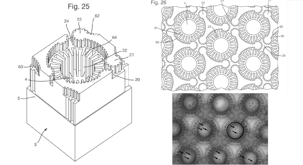
The text states that each well is ~90 microns deep, and that there is indeed a Platinum electrode at the base of the well, as we previously speculated. Structures shown here also closely match those shown in patents:
The book also describes routing connections to these electrodes through the sensor array silicon substrate, which sounds very much like a TSV process, as previously discussed.
Overall, this is a pretty awesome book containing details I’ve not seen discussed elsewhere. Well worth checking out!


